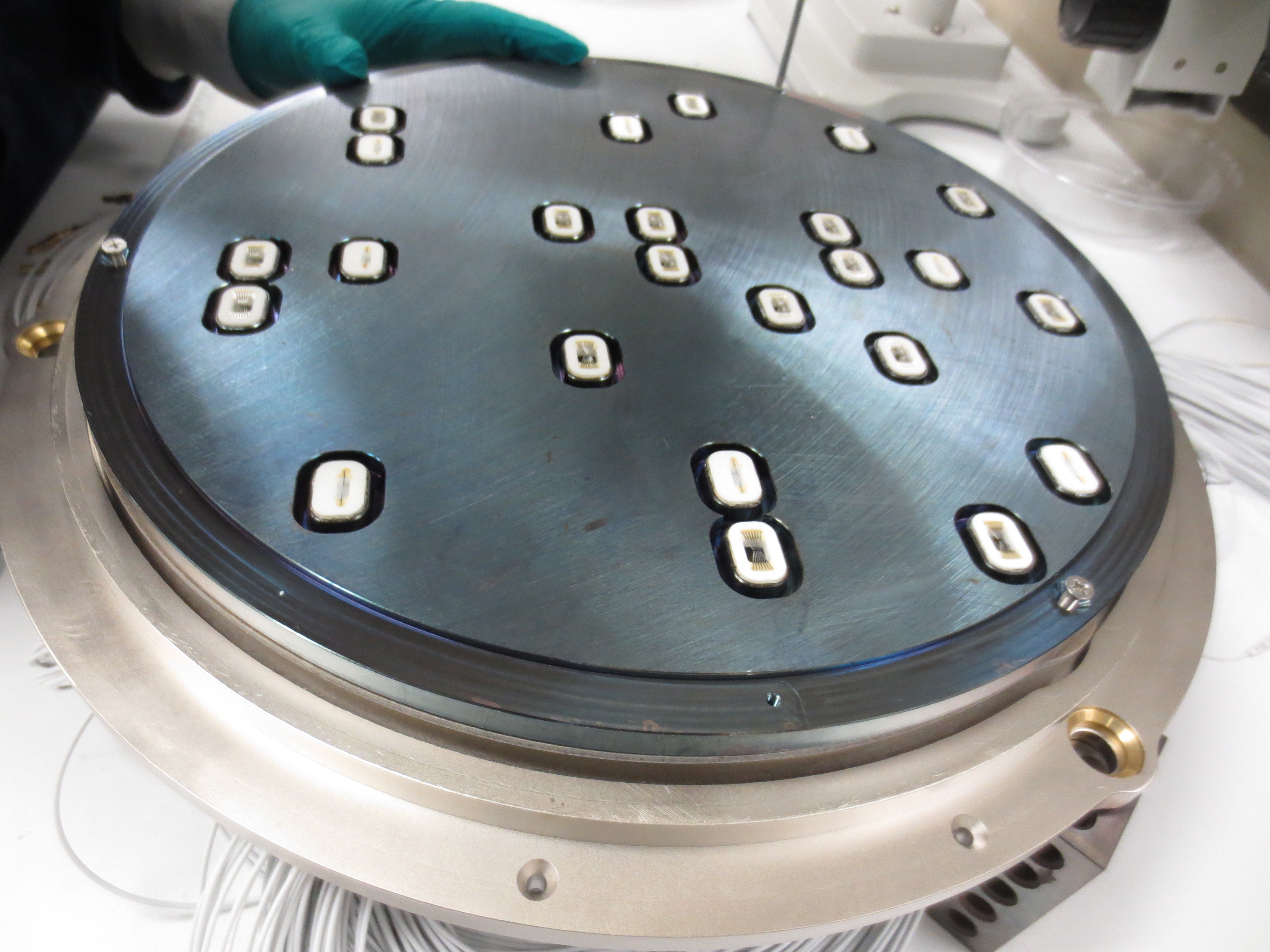
Q: Can I probe every device on the wafer?
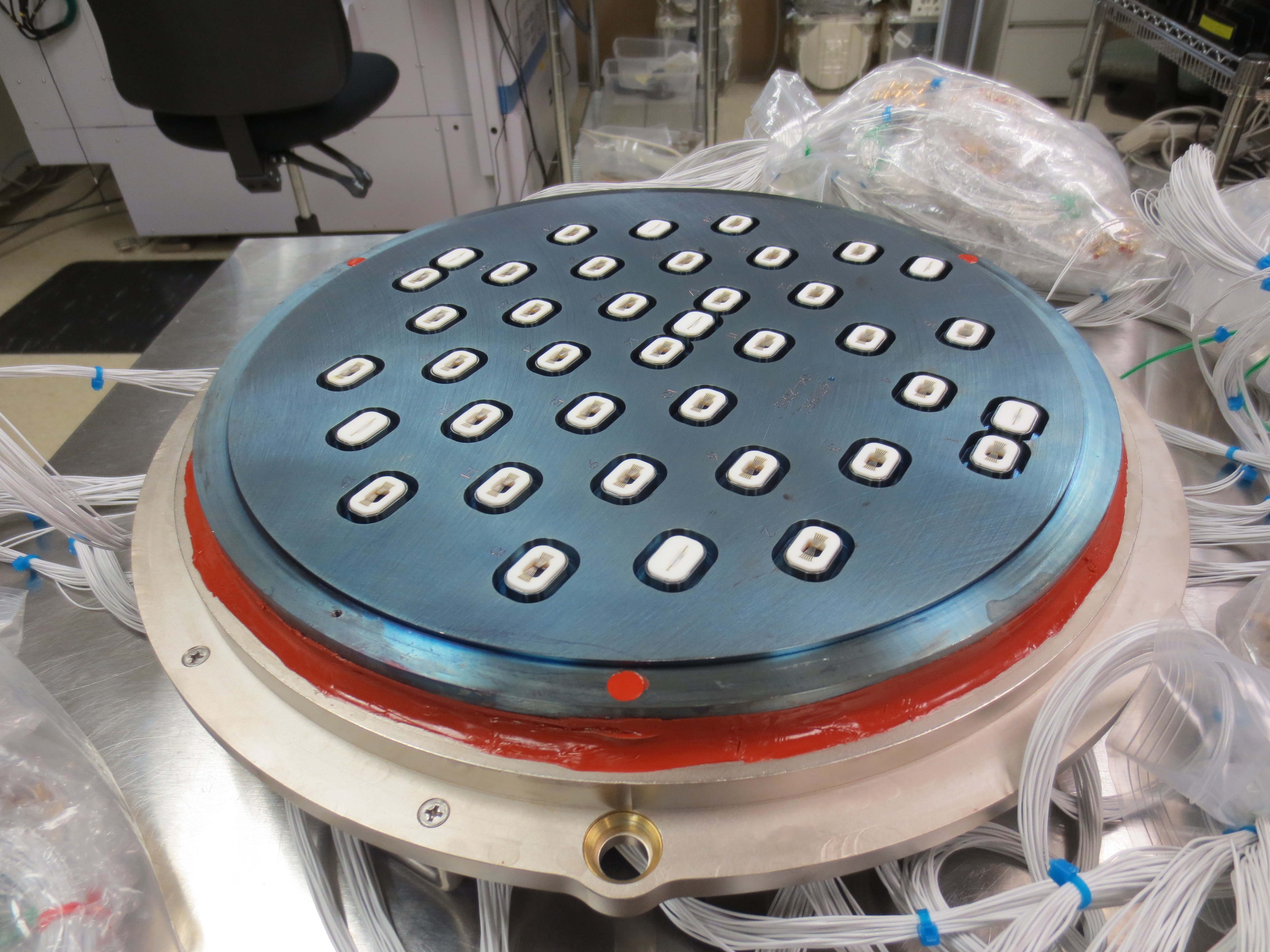
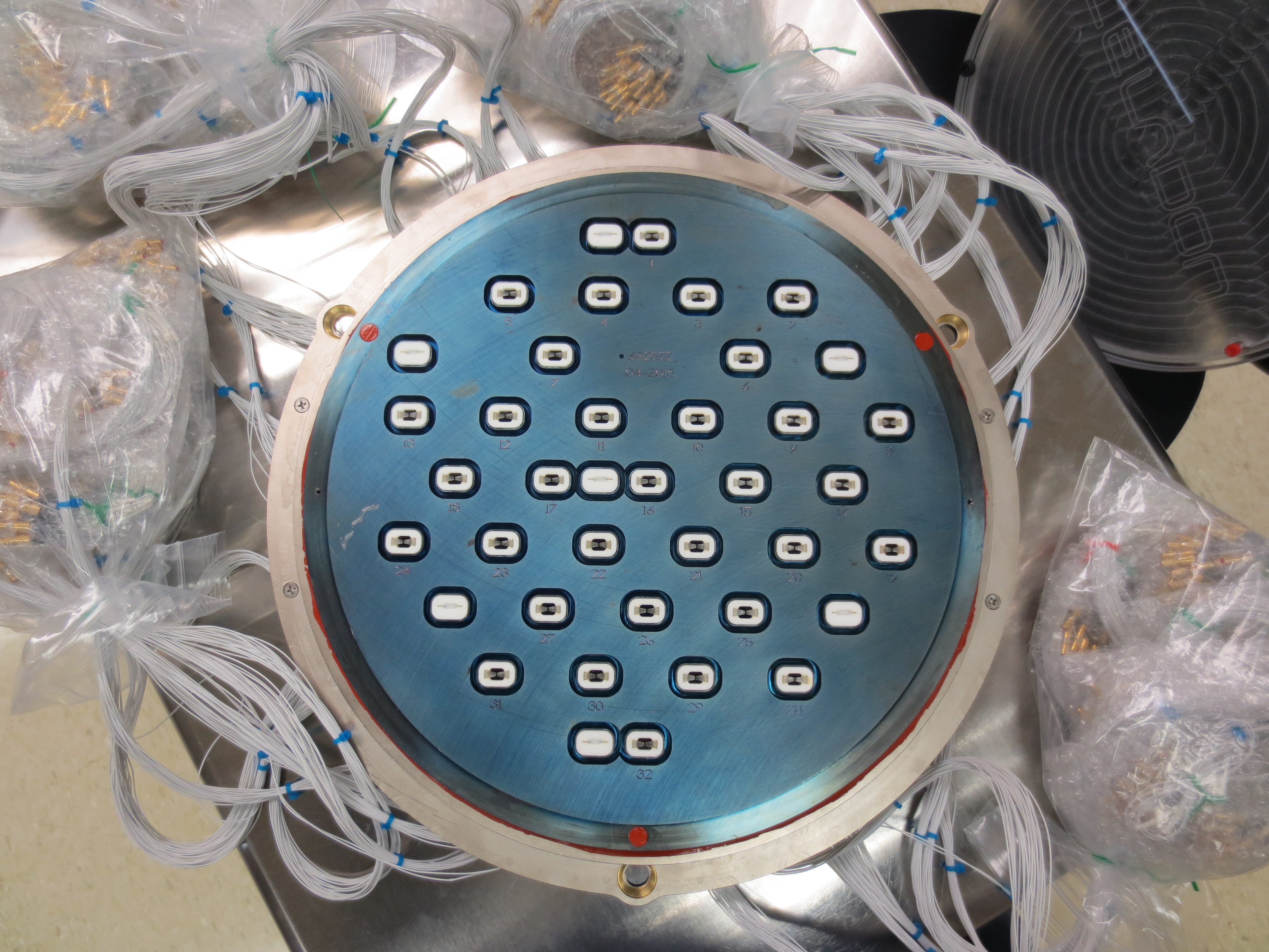
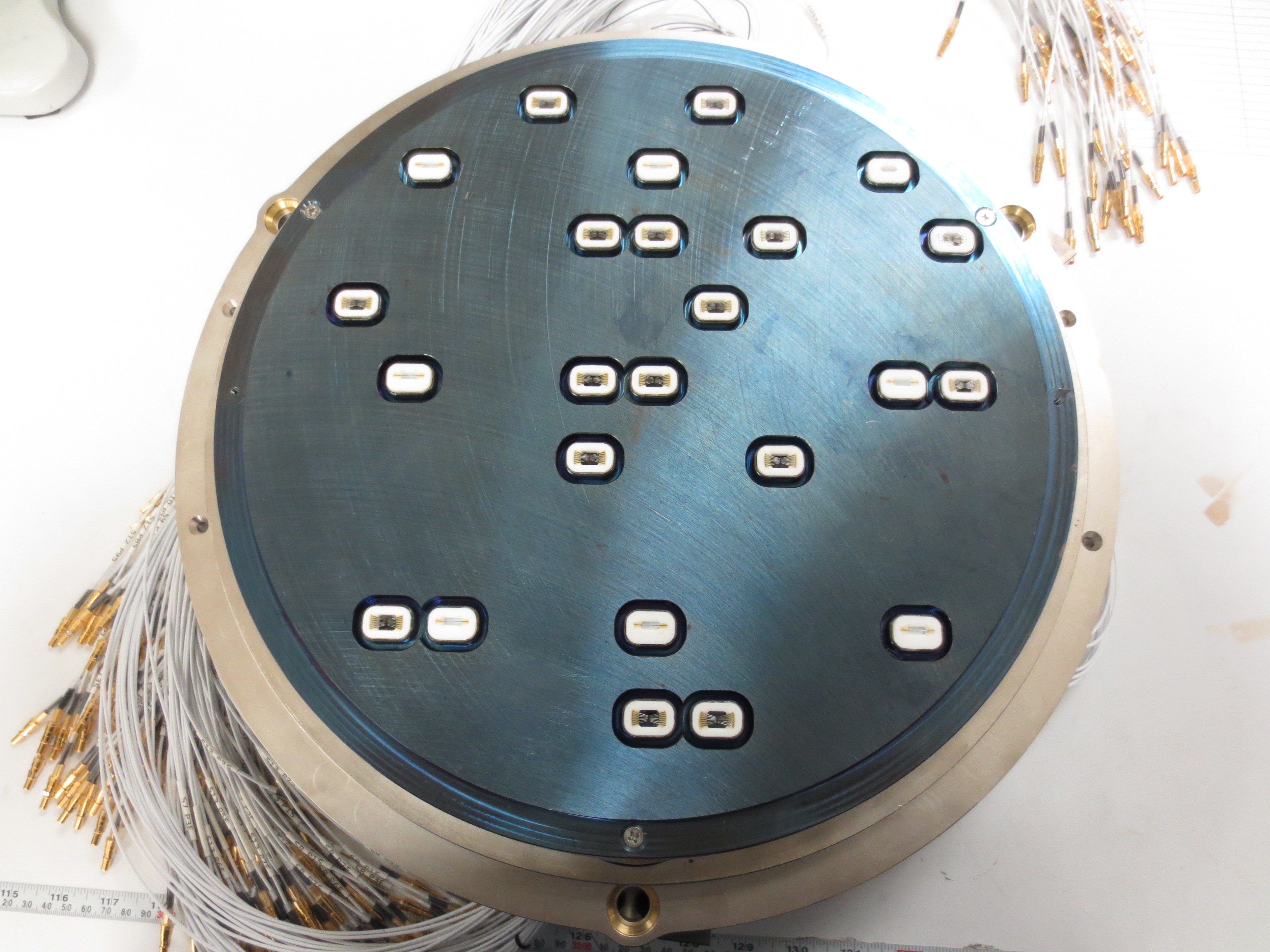
A: You can probe most of your devices on the wafer at the same time; the number depends on your device and wafer layout. You should not expect to probe every device on the wafer at the same time. The number of devices you probe depends on how much Z force your prober chuck can support, and how many channels your tester can support.
Q. What testers does Celadon support?
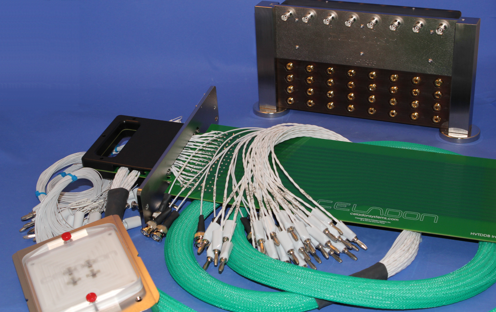
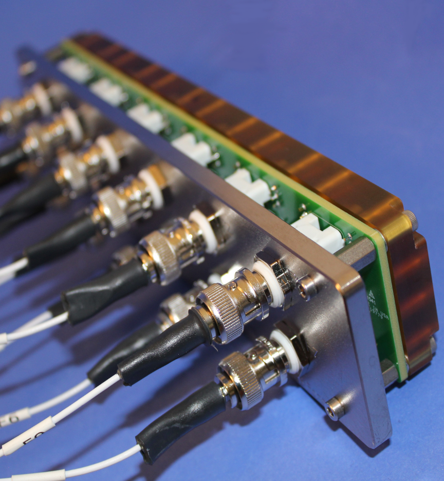
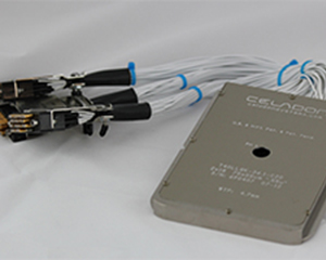
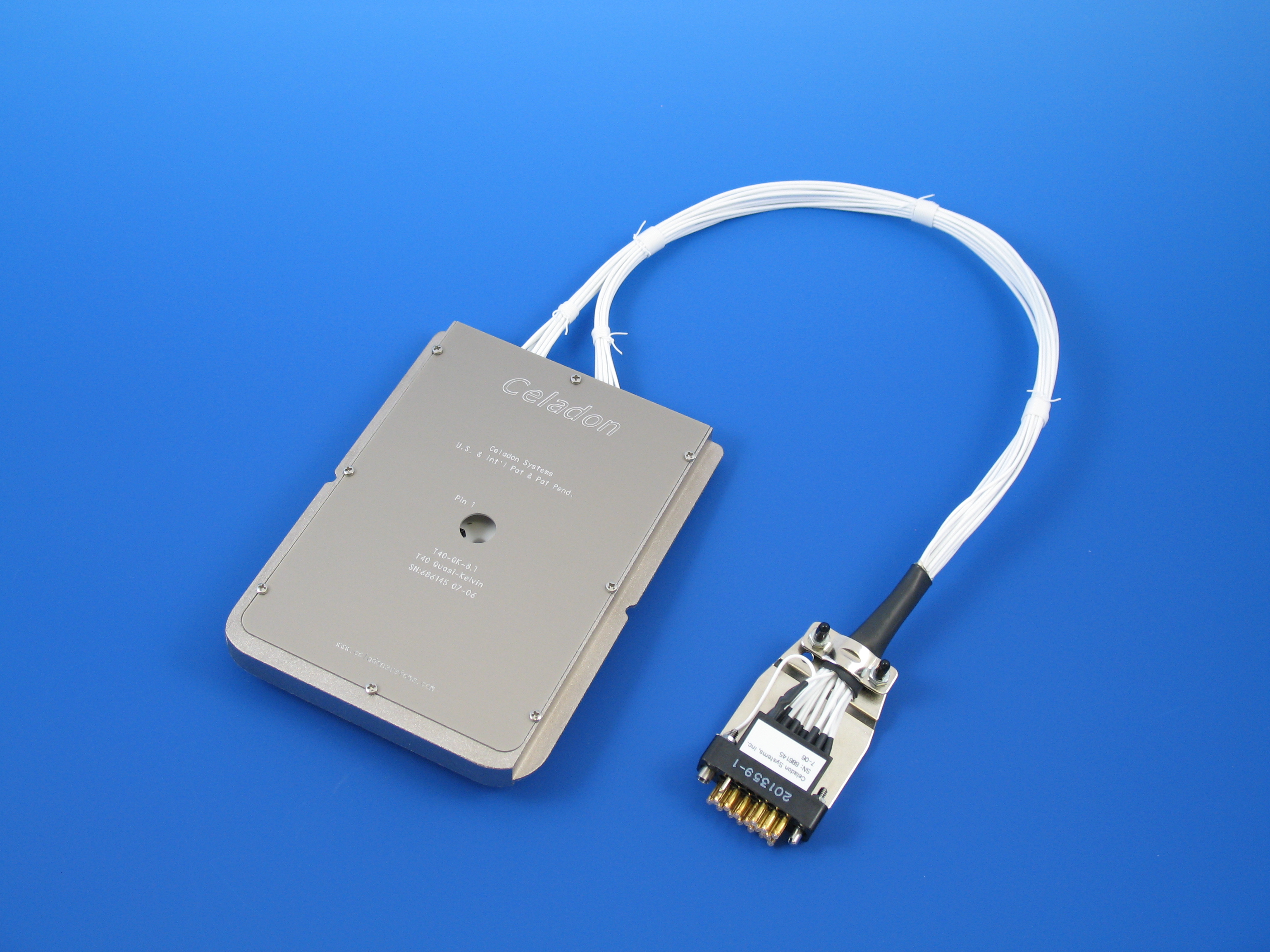
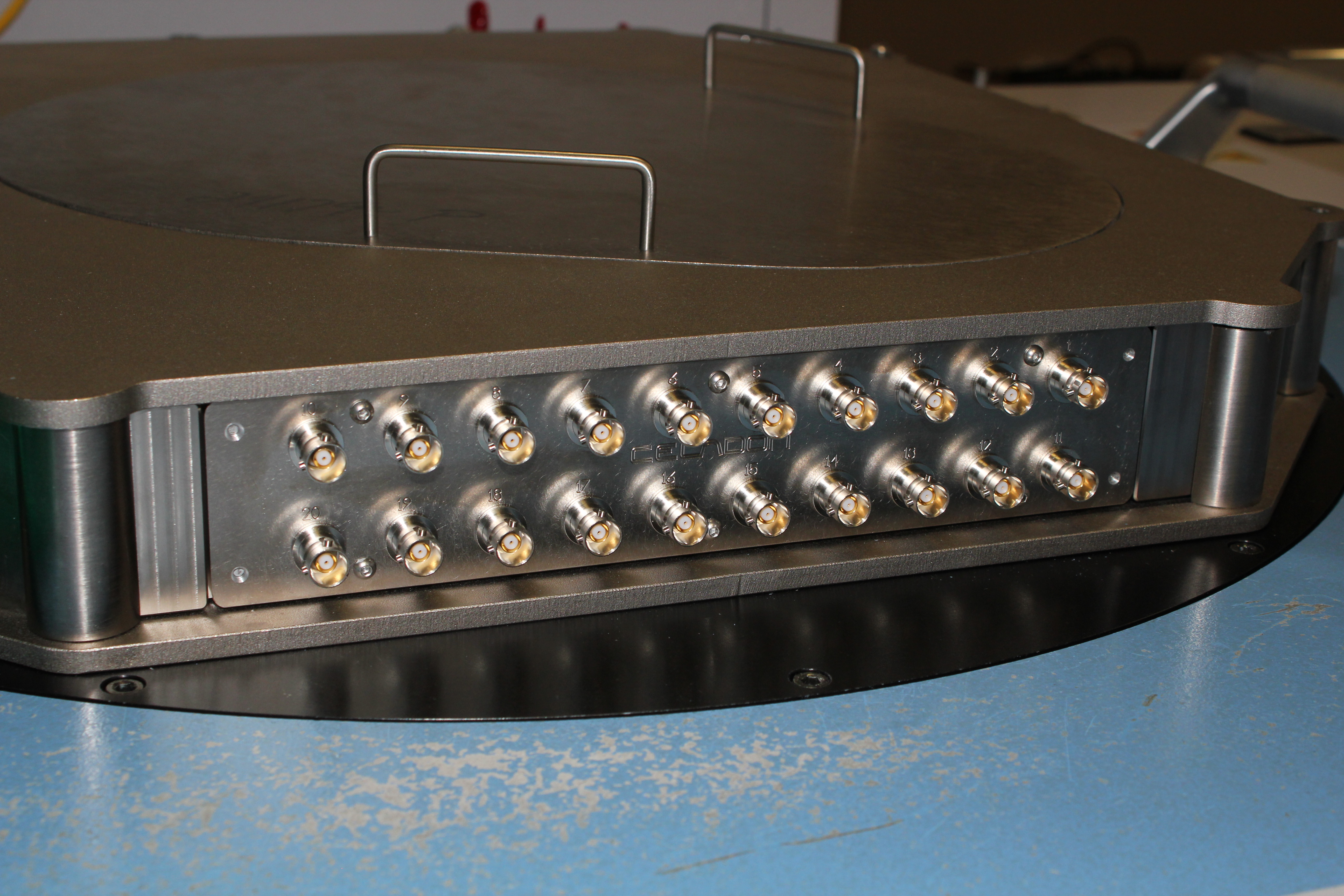
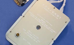
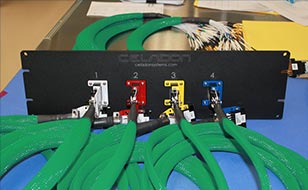
A. Currently, Celadon supports all industry standard parametric testers, reliability testers, parameter analyzers and switching matrices for DC measurements. Celadon manufactures interface cable assembly and custom interface boards to allow for this interconnection.
Q. What probers are Celadon Cards used on?
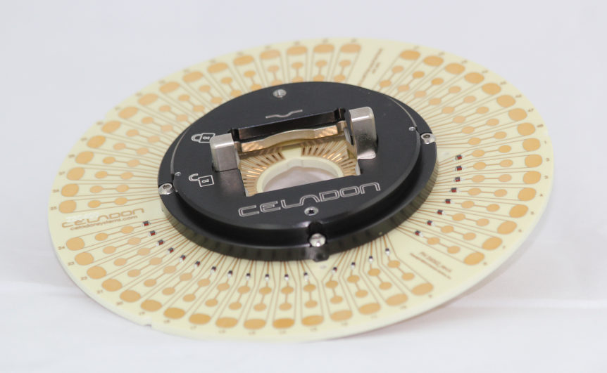
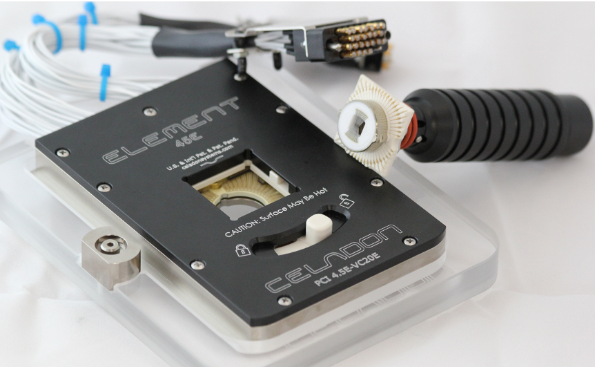
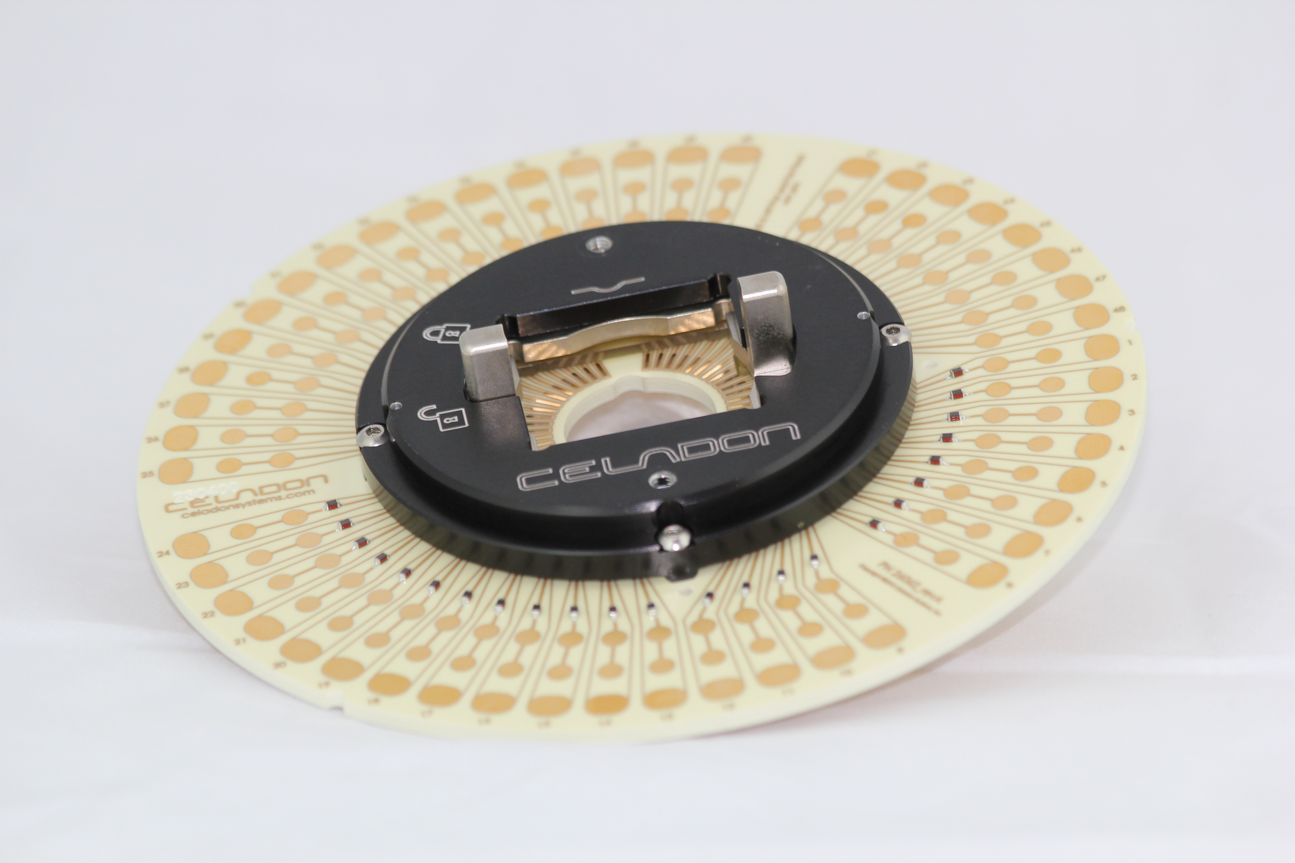
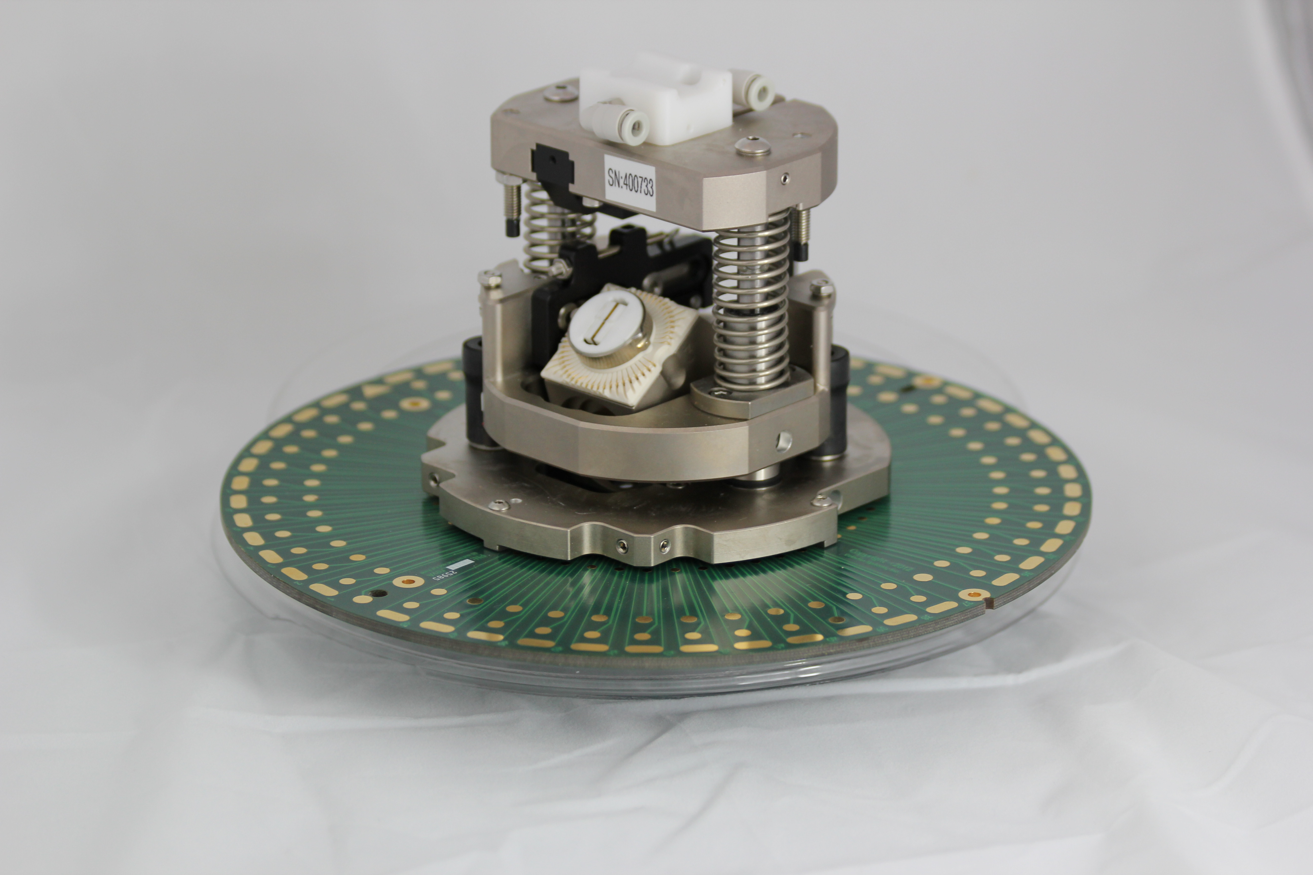
A. Currently, any 6” prober or larger that has a probe card holder, planarized chuck and optics that move to the furthest points to be probed will work. Single site probe cards such as the VersaTile™ with Advanced Cantilever™ technology can also be mounted on positioners that have planarization and theta adjustments. For low current measurements, a Faraday cage or dark box is required. Celadon does manufacture probe card holders or probe holding solutions for most brands of probers. While most probers can be used, multi-site probing often requires a Celadon probe card holder due to rigidity and planarization requirements.
Q: How many devices can I probe per probe tile?
A: You can expect to probe many devices per tile. Again, this ultimately depends on your layout. You will often find that you can probe more devices than you can test. The limiting factor is usually tester capacity and tester software.
Q: Is there a preferred bond pad size?
A: Certainly the larger the bond pad size the easier it is. The bond pad size needs to increase as wafer size increases to make up for mismatches in thermal expansion characteristics between a probe card and wafer which is dependent on total thermal test range. Due to Ceramic construction, Celadon Probe Cards have a very close match between wafer expansion and probe card expansion enabling users to just have one probe card to cover a whole temperature range. There is a relationship between maximum distances from pad to pad due wafer size, temperature range and pad size. Celadon application engineering can review this with you.
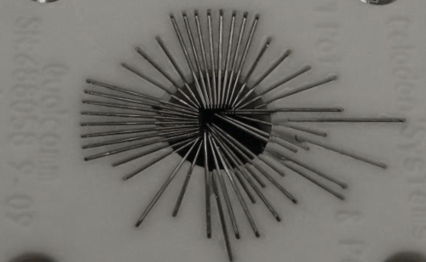
Q: What are the smallest bond pads the tiles can probe?
A: The smallest bond pads probed with a Celadon tile to date are 30 x 30 microns. Generally, maintenance costs and alignment times decrease with larger pad sizes. The product pages on the web site indicate minimum pad size for the maximum spacing for each probe card size for a temperature range. This is dependent on the prober positioning system and whether pattern recognition systems are used to ensure good probe-to-pad alignment.
Q: What is the minimum bond pad pitch?
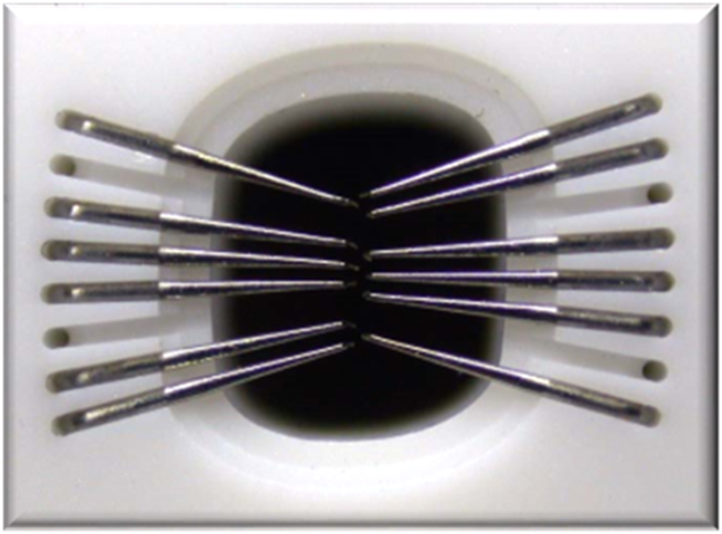
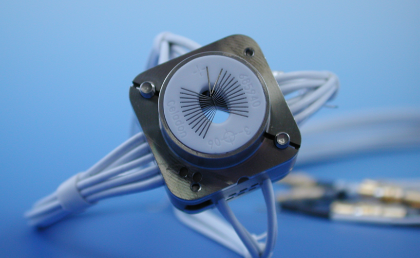
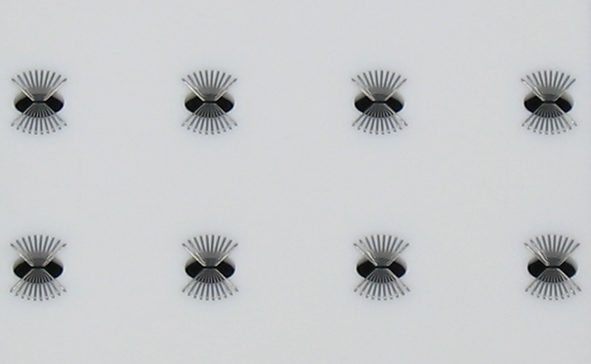
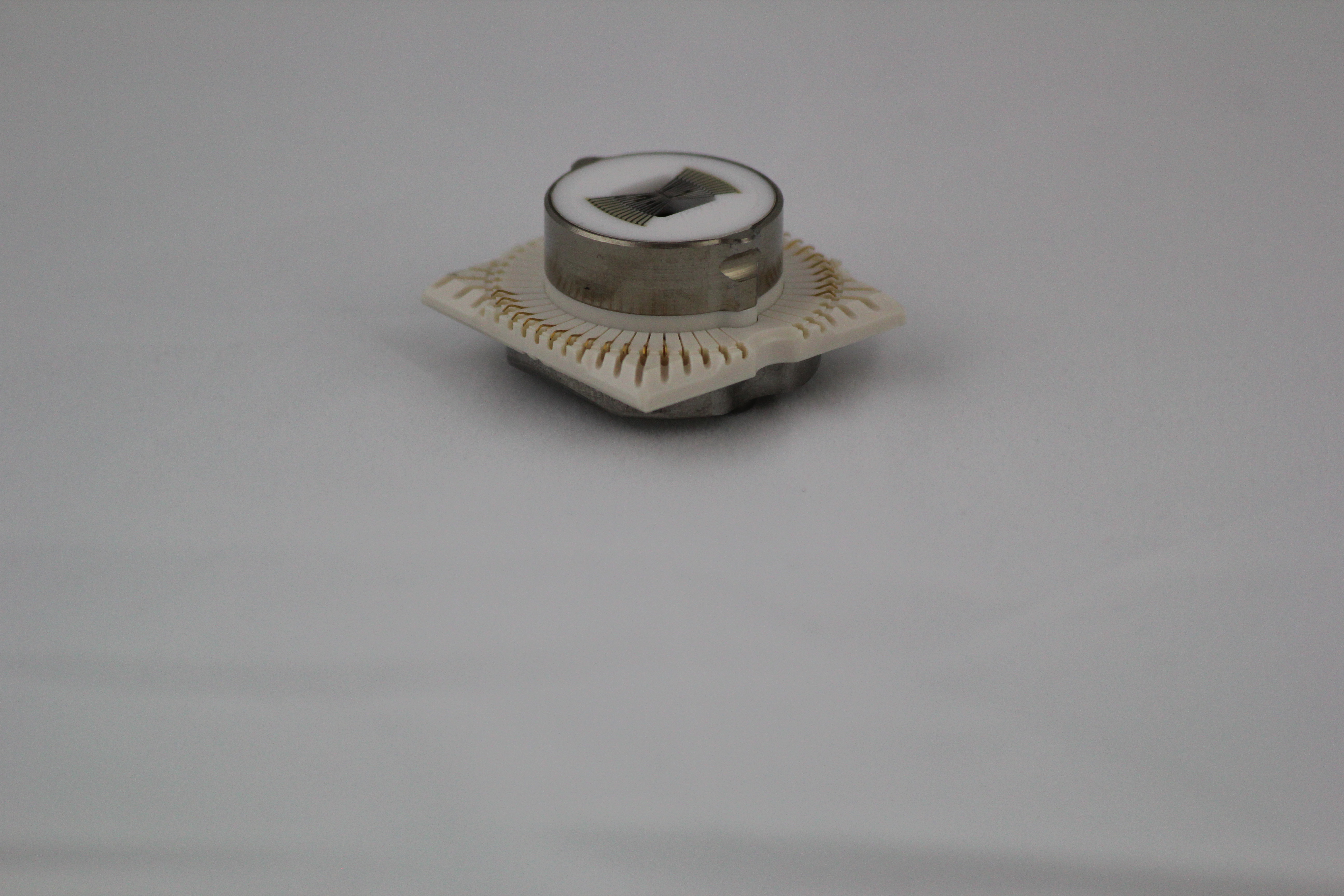
A: Celadon has built cards with pitches as low as 50 microns. Another interesting example was a probe card built for a 1 x 25 pattern with a 60 micron pitch pattern with two probes on each 40 x 60 micron pad for Kelvin probing. Celadon has made major progress in the ability to engineer probe cards for tight pitch probing.
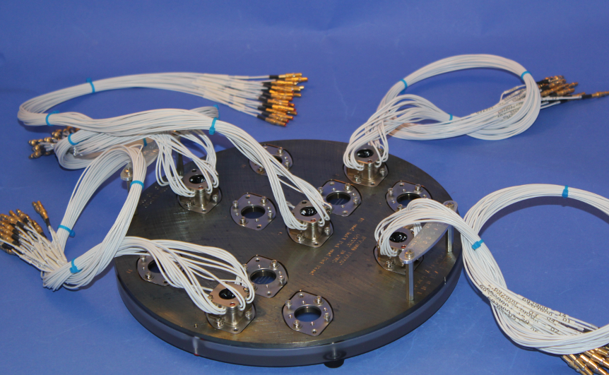
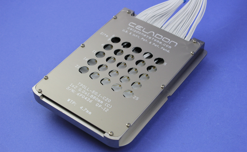
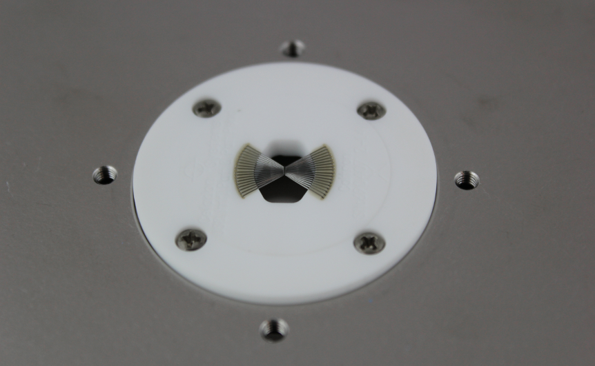
Q: Can the probe cards access bond pads configured in a grid or an array?
A: Yes. You can probe arrays, perimeters, 1 x n, or 2 x n patterns or N x N. Again, it specifically depends on your pattern. Contact us with your specific needs.
Q: How long do the tiles last?
A: With reasonable care, the tiles will last a very long time. There are some tiles that have been in use for more than 30,000 hours at temperatures of 250° to 300°C without any reduced performance. With 35 microns of overdrive on aluminum pads and proper cleaning and conditioning, many customers report 2,000,000 to 4,000,000 touchdowns. Probes last much longer on gold. Probe life is greatly affected by operator setup, wafer cleanliness, prober brand, and prober maintenance.
A probe will stop working or have high contact resistance if it is bent or broken, but it can be easily replaced. The probes are built for thousands of touchdowns. If the Celadon probes get dirty they are best cleaned with methyl alcohol and very light brushing with soft tooth brush.
Q: Can the tiles be repaired?
A: Yes. Individual probes can be replaced or easily re-aligned. With a Celadon probe card aligner and factory training, users can maintain some of the probe cards.
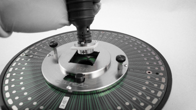
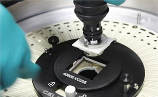
Q: How can you be sure the all the probes will touch?
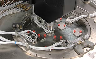
A: By planarizing the platen during initial setup. The chuck must be planarized and checked for flatness and room and under thermal conditions. Multi-site cards require chucks that are not warped. For the probes to contact each site, the prober must be required to compensate for temperature, wafer growth in each direction and possibly use probe to pad alignment if available. Proper stepping accuracy is becoming a big issue as pad sizes shrink. For multi-site cards, Celadon uses touch down sensors with a touch down sensor electronics indicator to indicate when all touch down sensors are in contact.
Q: Are low leakage measurements possible with Celadon tiles?
A: Yes. The pin to pin leakage has been measured at less than 5 femtoamps per volt at 25°C on a low leakage card. On an AttoFast ™, it is 1 femtoamp per volt. It is not specified for general purpose tiles or edge connector products.
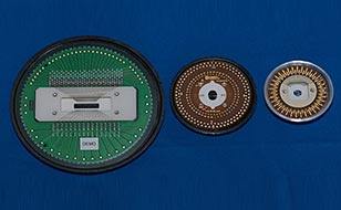
Q. Why is ceramic used instead of FR4 or Polyamide?
A. Ceramic makes extreme temperature range and low leakage measurements possible. Ceramic expansion rate is close to wafer thermal expansion rate unlike FR4 or polyamide, which are poor choices for high performance especially in high temperatures.
Q. Why does Celadon run cables directly to the probe instead of use edge connectors?
A. Running triax or coax cables to the probes directly prevents cross-finger leakage on materials that may be poor insulators. Settling time is faster. It is difficult to specify a leakage rate with FR4 and edge-mounted connectors and keep the connector surface clean enough for low leakage measurements.
Q: Are the Celadon probe cards truly unbreakable?
A: You will not break a tile if you over drive it onto the wafer under most conditions. The tiles will simply sit down on the wafer. However, if the wafer is aggressively driven into the tiles, there is a limit to what the wafer, chuck, tiles and platform will endure. If you drop it on the floor, it may break.
Q: How does the cost of a tile compare to polyamide probe cards or ceramic bladed cards?
A: The initial cost is higher but with one or two realignments, the cost of ownership is much less. First year costs are generally less and uptime is much higher due to the crash-resistant design. Celadon can quote probe cards with prepaid repairs for alignments and rebuilds so you can compare costs. Total test cost may be less when you consider ROI for Multi-Site cards. AttoFast™ cards with Celadon Triax cabling systems settle quickly which permits much faster die-to-die moves, which may eliminate having to purchase additional testers, which makes overall system and test costs much less than regular probe cards.
Q: How does the cost of a tile compare to package level testing?
A: The initial capital cost is higher for wafer level. However, over time, factoring in packaging costs, DUT board costs, and the speed with which you obtain the results, wafer level costs much less. The biggest overall cost is end product time to market.
Q: Does this mean all my probe cards are obsolete?
A: Absolutely not. But if you need to do low leakage measurements, multi-site probing, or high temperature testing, Celadon tiles are the best solution.
Q: What is the typical lead time?
A: Call us for details. Repeat designs are faster because the design capture is already completed.
Q: How much does it cost?
A: The price depends on the number of probes, tile size, cable and the number of tiles. Call for a specific quote.