

Press Release

Celadon is excited to announce that we have made it into the Top 64 entries in the Minnesota Chamber of Commerce’s “Coolest Thing Made in Minnesota” competition! We were nominated for our Ultra-Cold Testing Solutions for Quantum Computing, AI, Space Travel, and other super cool Cryogenic Semiconductor applications.
Celadon makes customizable electrical test setups that include high performance probe cards, circuit boards, and cables designed to test semiconductor devices at temperatures below -452 degrees Fahrenheit, which is almost as cold as possible! Our setups are being used by some of the most advanced semiconductor companies in the world to push the boundaries of technologies that are shaping the future.
We’d greatly appreciate your support as we proceed in the competition. First round voting is from September 3 at 12:00 pm through September 8 at 11:59 pm. During that time, you are allowed to cast one vote, per email, per day, per match up. #CoolestThingMN

WLR Product Advancements from MPI Corporation & Celadon Systems Inc.
San Jose, CA, March 17th, 2022
“We have admired Celadon’s technology and measurement prowess for many years now,” says Stojan Kanev, General Manager of the Advanced Semiconductor Division of MPI, “and are honored to provide complete solutions with our combined strengths. With the cross-pollination of technologies and talent, we are providing an even higher level of value to the Wafer Level Reliability market.”
“It has been a privilege for the Celadon team to work with such a high caliber talent within the Advanced Semiconductor Test Division of MPI, a leader within the WLR market,” says Karen Armendariz, President of Celadon Systems, “The natural synergies between our organizations have accelerated the joint development efforts. Together, we are excited to offer one-of-a-kind solutions to our WLR customers.”
For more information, please visit us at the International Reliability and Physics Symposium (IRPS) booth #104 on March 27th – 31st, 2022 in Dallas Texas. Hope to see you there!
About MPI Corporations
Founded in 1995 and headquartered in Hsinchu, Taiwan, MPI Corporation is a global technology leader in Semiconductor, Light Emitting Diode (LED), Photo Detectors, Lasers, Materials Research, Aerospace, Automotive, Fiber Optic, Electronic Components and more. MPI’s four main business sectors include Probe Card, Photonics Automation, Advanced Semiconductor Test and Thermal Divisions. MPI products range from various advanced probe card technologies, probers, testers, material handlers, inspection and thermal air systems. Many of these products are accompanied by state-of-the-art Calibration and Test & Measurement software suites. The diversification of product portfolio and industries allows a healthy environment for employee growth and retention. Cross pollination of product technologies allows each new innovation to provide differentiation in areas that are meaningful to our MPI America Inc., 2360 Qume Drive, Suite C, San Jose, CA 95131 precious customer base. For more information please visit: www.mpi-corporation.com
About Celadon Systems Inc.
Celadon Systems, Inc., The Home of Peace of Mind Probing, was founded 1997 by Bryan and Valerie Root and is headquartered in Burnsville, Minnesota. Celadon Systems is focused on the design and manufacturing of advanced probe card solutions and high-performance cables. Celadon Systems is a global leader in parametric test, wafer level reliability, modeling, characterization, cryogenic applications, and high-power probe cards for the semiconductor industry. As an industry leading, on- wafer probing solutions provider, Celadon’s reputation for delivering ultra-high performance probe cards that thrive in extreme temperatures is unparalleled. Celadon seeks to enrich the lives of our customers, employees, and community partners by offering a challenging, inspiring, and empowering environment that drives strong and profitable growth. For more information, please visit: www.celadonsystems.com
Contact:
Elaine Chuang
Karen Armendariz
Celadon Invests for Growth
Without question, 2020 was an unprecedented and challenging year for many companies for a variety of reasons beyond the pandemic. Fortunately, the semiconductor industry has been thriving due to WFH, 5G, AI, Cloud, etc., which drives the need for silicon, and, we at Celadon, feel lucky to be a part of this industry and the associated growth. We used 2020 as an opportunity to continue to build our infrastructure. Celadon focused on increasing our capacity and resilience through equipment, people, and software investments.
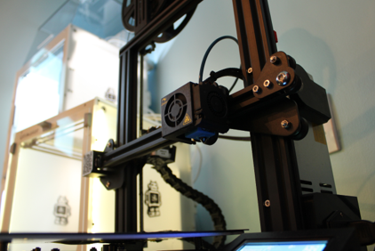
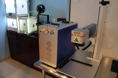
In response to increased probe card demand, our team has increased our staff by over 15% and we have plans to continue to grow in engineering and manufacturing in 2021. In 2020, we doubled our ceramic output through key capital equipment investments; previously ceramic milling was our bottleneck to significant growth. We also invested in 3D printers which have been integral in reducing time-to-market of our products including “specials” and other custom solutions. These systems have been instrumental in reducing costs and have been useful in supplementing the manufacturing process of some of our products. Among other new equipment, we also acquired a new laser which allows us to add additional features to our products and packaging. Manufacturing floor automation began in 2020 and will continue throughout 2021. Through significant software and hardware investments on the floor, we are streamlining our processes, communication, and ultimately, our lead times.
We are extremely excited to be able to support our customers and partners as they continue to grow. We expect 2021 to be a another year of growth in our industry.
Celadon Systems to host first CORE Virtual Users’ Group!
About this Event
Celadon Systems is excited to invite you to join us virtually on March 24th for an interactive forum bringing our users together to discuss challenging on-wafer probing applications and solutions.
We are very appreciative of our customers from the fabs, labs, and test floors, who will be presenting on the following topics over the first half of the program with live Q&A:
Customer Speaker Topics:
“Celadon Probe Card – lifetime, cost & dependability” (Texas Instruments)
“Hot Cantilever Probe Setup Optimization” (Allegro Microsystems)
“Leveraging the Multisite rail system for intrinsic reliability qualification on discrete power and analog Integrated circuits” (On Semiconductor)
“Deep Trench Probing using Celadon VC20 Probe card” (Sandia)
“Temperature Testing using Celadon VC20 Probe cards and Motherboards” (NXP)
“Are Celadon Probe Cards the right choice for me” (A review of Celadon’s new cost of ownership model jointly prepared with experienced customers.)
The second half of our event will include interactive, video-based, topic specific Chat Rooms. These Chat Rooms will be staffed with experienced customers and/or Celadon engineers:
Chat Room Topics:
Optimizing Lifetime Performance in Production Using Celadon Probe Cards
Over Temperature Probing Using the VC20™ on Very Small Pads
Single-Site High Temperature Probing – T40’s and VersaTile’s
WLR/Burn-in Multisite Probing
Production Multisite Probing
Cryogenic Probing
High Voltage Probing
General Probing Applications Including Positioner Based Probing, ESD and Magnetic Applications
Please register soon! We look forward to “seeing” you all there. Thank you from your Team at Celadon.
Interested in attending?
Submit a request for an invitation below:
Press Release: Bryan Root, Founder, and Owner of Celadon System’s, Inc., has been elevated to an IEEE Fellow
 Mr. Root is a pioneer and key innovator in semiconductor wafer level test. His revolutionary work spans 35 years and is used by more than 300 semiconductor companies and institutions in labs, fabs and test floors around the world today. In reliability and device test, he has been a key researcher, inventor, developer, implementer, evangelist, manufacturer, and a driver of industry standards. These contributions touch every device manufactured by the industry. Manufacturers report quicker time to market by eliminating packaging before testing, reducing test time and time to test, and reducing the cost of test. Mr. Root’s work has quickened the pace of the industry by lowering costs and improving device functionality and reliability.
Mr. Root’s contributions began in 1984 when he started his research on methods to assess the reliability of devices and structures at the wafer level. His research focus was to accelerate semiconductor reliability testing from weeks to days or even seconds. This required new test methods and improving existing test methods. The result of his significant body of work has been his invention of SWEAT (the Standard Wafer-level Electromigration Accelerated Test), a breakthrough in semiconductor reliability testing that ushered in the era of Wafer-Level Reliability (WLR) characterization, and for the first time, thin film metallization reliability testing could be incorporated as a monitor in the manufacturing process flow; his refinement and popularization of the Isothermal test (a fast wafer level electromigration test); and the invention and development of equipment and probe cards for parallel large sample size wafer level reliability tests. Additionally, through Mr. Root’s founding and leadership of the JEDEC 14.2 standards committee on wafer level reliability, he drove the standardization and popular use of tests for electromigration (contributing his own work on SWEAT and the Isothermal test), TDDB (Time Dependent Dielectric Breakdown) and, HCI (Hot Carrier Injection). With the foundation of these standards in the public domain, and the adoption by other standards organizations like JEITA, researchers continue to refine and publish new work. To add to this impressive list of accomplishments Mr. Root’s pioneering work beginning in 1987 resulted in the first commercially successful equipment for electromigration, TDDB and HCI test and this equipment continues to be widely used in the semiconductor industry.
In 1997, Mr. Root shifted his focus to solving the theretofore insurmountable industry problem of precisely and reliably probing and measuring electrical parameters on wafers under extreme conditions. Mr. Root’s inventions and 66 patents are now widely used in the industry and have resulted in the only full wafer (200mm and 300mm) crash resistant multi-site massively parallel test probe cards for reliability and burn-in, capable of sustained use up to 400°C, some of which have endured continuous use at temperatures above 250°C for several years; invented the first crash resistant, low current leakage (fA), low EMI noise, device and reliability test probe card capable of long term sustained use at -65°C to 400°C; invented the first device test probe card for sustained use at 600°C ; invented the first fast-settling ultra-low current leakage (sub 1 fA/V at 23°C and sub 10fA/V at 300°C) probe card for long term sustained use at temperatures of -65°C to 300°C; invented the first small format low-leakage, crash resistant, 4K to 300°C probe card for single site or multi-site use in device test or reliability test; invented the first low leakage low noise quick-swap parametric probe core; invented the first parametric probe card indexer for swapping cores in seconds enabling “lights out” in situ diagnostics; invented the first non-magnetic close-coupling, swappable, probe core for ultra-high magnetic field (up to 0.8T) testing; invented the first high voltage(3000V) 23°C to 200°C swappable core utilizing a temperature controllable air jet for pressure and turbulence to suppress surface arcing; invented an ultra-stable functional test probe card for sustained use at high temperatures. Today, tens of thousands of Mr. Root’s ultra-reliable mission critical probing solutions are widely in use today worldwide by nearly all semiconductor companies, foundries, medical device companies, space and military companies, universities and research institutes. Within these companies the critical and essential probing solutions are found in reliability labs, ESD labs, modeling and characterization labs, burn-in labs, as well as production parametric and functional test floors.
Mr. Root’s seminal work in Wafer-Level Reliability was initiated at Mostek as a device reliability engineer, continued at Sperry as a senior device engineer, accelerated with the founding of Sienna Technologies, and continues today after he founded Celadon Systems in 1997. Mr. Root continues to mentor and fund young engineers and interns in high voltage device and reliability test and RF reliability research.
At Mostek, Mr. Root initially worked on developing a test for thin film electromigration susceptibility. He was the lead researcher in the discovery and development of SWEAT (the Standard Wafer-level Electromigration Accelerated Test). Conventional Electromigration testing at the time was costly and time consuming. Ovens were typically required to apply high temperatures to packaged devices to accelerate failure. The tests typically took many weeks to obtain results. SWEAT uses very high current densities to achieve tightly controlled joule heating derived from the measured resistance to accelerate failure in seconds. The test could be conducted at the wafer-level saving significant costs associated with packaging. This was a breakthrough in semiconductor reliability testing. Mr. Root went on to further refine the SWEAT algorithm and “bowtie” test structure that enhances current crowding. Mr. Root also contributed the algorithm to international standards organizations and SWEAT is now part of a standard software toolkit for manufacturers. Google Scholar shows more than 250 publications that reference the technique.
In 1987 Mr. Root was invited to start a JEDEC (Joint Electron Device Engineering Council) working group to develop international standards, processes and publications for wafer level reliability tests. The rapid success of the working group resulted in JEDEC elevating it to a full “point” committee: JC14.2. Mr. Root organized JC14.2 into three subcommittees, electromigration, TDDB, and, Hot Carriers, and recruited the leading industry authorities to the subcommittees, attracting 30 to 40 industry authorities across broad sectors of the industry to contribute their expertise and attend the meetings. Mr. Root also contributed his algorithms for SWEAT and the Isothermal Test as well as test structures. JC14.2 published several standards and methods while he was the chairman and continues to do so today. These standards are used world-wide by the semiconductor industry to routinely characterize semiconductor device reliability and are referenced by other international Standards organizations like IEC, and JEITA.
In 1997 Mr. Root focused his research on reducing time required to obtain conventional reliability data by performing all testing on the wafer. Alone, in his basement, he invented a totally new ceramic probe card technology to perform massively parallel conventional reliability tests at the wafer-level, eliminating the need for packaging test structures. In reliability, the Celadon Ceramic probe card is used to test hundreds of devices in parallel on a single wafer at temperatures from room temperature to 400°C. Several major semiconductor companies use the Ceramic probe card to obtain conventional reliability data and report saving millions of dollars each year in packaging costs alone. Additionally, Mr. Root’s invention allowed “wafer level burn-in” to become a reality. Now there are companies that burn-in entire wafers of integrated circuits without costly packaging. In device and parametric test, Mr. Root invented a highly reliable, easy-to-swap, long lived, ceramic probe core that is widely used in the industry today and has improved the quality of the data and reduced the cost of test at numerous leading semiconductor companies and many others by hundreds of thousands of dollars on each test floor each year.
Today, as a result of Mr. Root’s pioneering work, SWEAT continues to evolve. SWEAT is also an indispensable tool at semiconductor manufacturers to quickly assess the reliability of vias that connect different layers of metal on an integrated circuit. It is common for these circuits to have 10 separate layers of metal or more, all electrically connected with vias. By monitoring the reliability of the vias, defective wafers are quickly identified preventing defects from continued processing or from reaching the field.
The JEDEC 14.2 committee was highly influential during Mr. Root’s leadership, directly benefiting the industry due to the high participation rate of industry experts and broad industry adoption of the publications and standards. He was both a technical contributor and organizational leader. This is a list of many of the standards and publications published by JEDEC 14.2: JEP-119, JEP-128, JEP-139, JEP-159, JESD-28, JESD-28-A, JESD-33, JESD-34, JESD35, JESD-35-1, JESD-35-2, JESD-37, JESD-60, JESD-61, JESD-63, JESD-87, JESD-90, JESD-92, JESD-202, JP-001.01. International organizations adopting the 14.2 work: JEITA, IEC.
Mr. Root’s revolutionary ceramic probe card invention in 1997 enabled an entirely new class of reliability testing and device burn-in. His massively parallel ultra-reliable probe cards enabled the ability to test at high temperatures up to 400°C. His inventions are extensively used at companies around the world to test in parallel for electromigration and TDDB reliability as well as full wafer burn-in. Si and SiC high temperature integrated circuit manufacturers burn in more than one thousand devices in parallel at the wafer level. Additionally, automotive component manufacturers use Mr. Root’s inventions to test and burn-in engine sensors to 600°C. Further, Mr. Root’s invention of the massively parallel ceramic probe cards enable the Automotive industry today to qualify their processes to 275C.
In 1998 Mr. Root extended his ceramic probe card research to develop the first highly reliable probe card for device modelling and characterization, with standard operating temperatures of -65°C to 300°C and ultra-low leakage making the probe card electrically invisible to the tester. The successors to this invention are used in labs everyday currently at most leading semiconductor companies. The Celadon ceramic technology and guarded probe AttoFast technology is used as a benchmark for device modeling and characterization between labs due to its broad acceptance.
In 2009 Mr. Root developed a probe core called the VC20 that could be quickly swapped and locked into a motherboard. The current version of this core is used extensively for production parametric test at numerous leading semiconductor companies. Its high reliability has reduced the direct probe card cost by a factor of 4 to 10 depending on the application. In 2010 in collaboration with a leading semiconductor company, the core was modified and mounted on an Indexer ushering in software controlled, automatic in-situ core changes – another first in the semiconductor industry. The Indexer further reduces cost of test by eliminating the need for test floor personnel to physically open up the test head to change the probe card, resulting in a “lights out” approach to wafer test never seen before by the Industry.
Webinar: Integrated Probe Card Solutions for Magnetic Testing
We discuss combining GMW’s expertise in Electromagnets & Magnetic Modeling with Celadon expertise in Probe Cards & Testing for complete integrated solutions compatible with all Probers. The fully integrated probe card is typically used for on-wafer parametric tests, modeling, characterization and wafer level reliability as well as functional tests.
Speakers:
- Tom King, Ph.D. | Lead Magnet Scientist | GMW Associates
- Karen Armendariz | CEO | Celadon Systems
- Bill Funk | Chief Technical Officer | Celadon Systems
Supporting Materials:
Originally recorded on August 26, 2020
Webinar: Integrated Probe Card Solutions for Magnetic Testing
We invite you to join us for a webinar on Tuesday, August 25 at 1pm PDT/4pm EDT. We will discuss combining GMW’s expertise in Electromagnets & Magnetic Modeling with Celadon expertise in Probe Cards & Testing for complete integrated solutions compatible with all Probers. The fully integrated probe card is typically used for on-wafer parametric tests, modeling, characterization and wafer level reliability as well as functional tests.
Speakers

Tom King, PhD
Lead Magnet Scientist
GMW Associates
Tom has an experimental physics background and has worked in the areas of laser physics, quantum computation and superconductivity. Since switching to commercial work, Tom has designed superconducting and copper magnets for industry applications. These include Hard Disk Drive testing systems, Ion implantation beam lines and MRAM test. Work with GMW started in 2006 and continues to the present.

Karen Armendariz
CEO
Celadon Systems
Karen Armendariz has over 25 years of experience in the semiconductor industry. Celadon Systems, Inc., is a US based industry leading on wafer probing solutions provider focused on the design and manufacturing of advanced probe card solutions, high performance cables and adaptors. Karen has held a variety of leadership positions throughout her career in manufacturing, engineering, and sales and marketing at Intel Corp., Cyrix, National Semiconductor, Creation Technologies and TEXSource, a leading manufacturer’s rep firm in the semiconductor industry. She holds a Bachelor’s Degree in Electrical Engineering from the University of Oklahoma and a Master’s in Business Administration from Oklahoma City University.

Bill Funk
Chief Technical Officer
Celadon Systems
Bill has enjoyed a life-long passion to design and build. With an Aerospace engineering degree from University of Minnesota, Bill worked the first half of his career with Beech Aircraft and Rosemount Aerospace. He then spent a few years doing factory automation and medical consulting. Bill finally joined Celadon Systems founder Bryan Root in his Basement, 20 years ago, to help build Celadon.
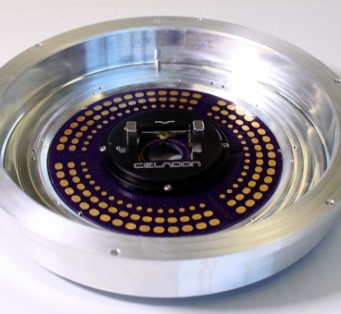
Electromagnet and Probe Station Integration
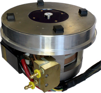
An example of the collaboration between GMW and Celadon System is the GMW 5207 Projected Field Electromagnet and Probe Station Integration to optimize the performance of the combined electromagnet and probe card.
- 5207 Electromagnet with custom Magnetic Pole Extender integrated with a Celadon Non-Ferrous VersaCore™
- Peak Field, Continuous (35A): >1.3T
- Peak Field, Triangle (60A): >2T
- Single device or 4 x 4mm whole array testing
- Celadon cards are compatible with any probe station
Additional Information
We will be discussing this integration along with other capabilities of GMW Associates and Celadon Systems on Tuesday, August 25 at 1pm PDT/4pm EDT.
June 29, 2020
Celadon Systems, Inc., “The Home of Peace of Mind Probing”, has partnered with GMW Associates to develop an innovative integrated electro-magnet and probe card solution. Using this unique configuration device testing of a single DUT with magnetic fields up to 1.0 Tesla is possible and up to .85 Tesla can be applied to an array.
May 22, 2020
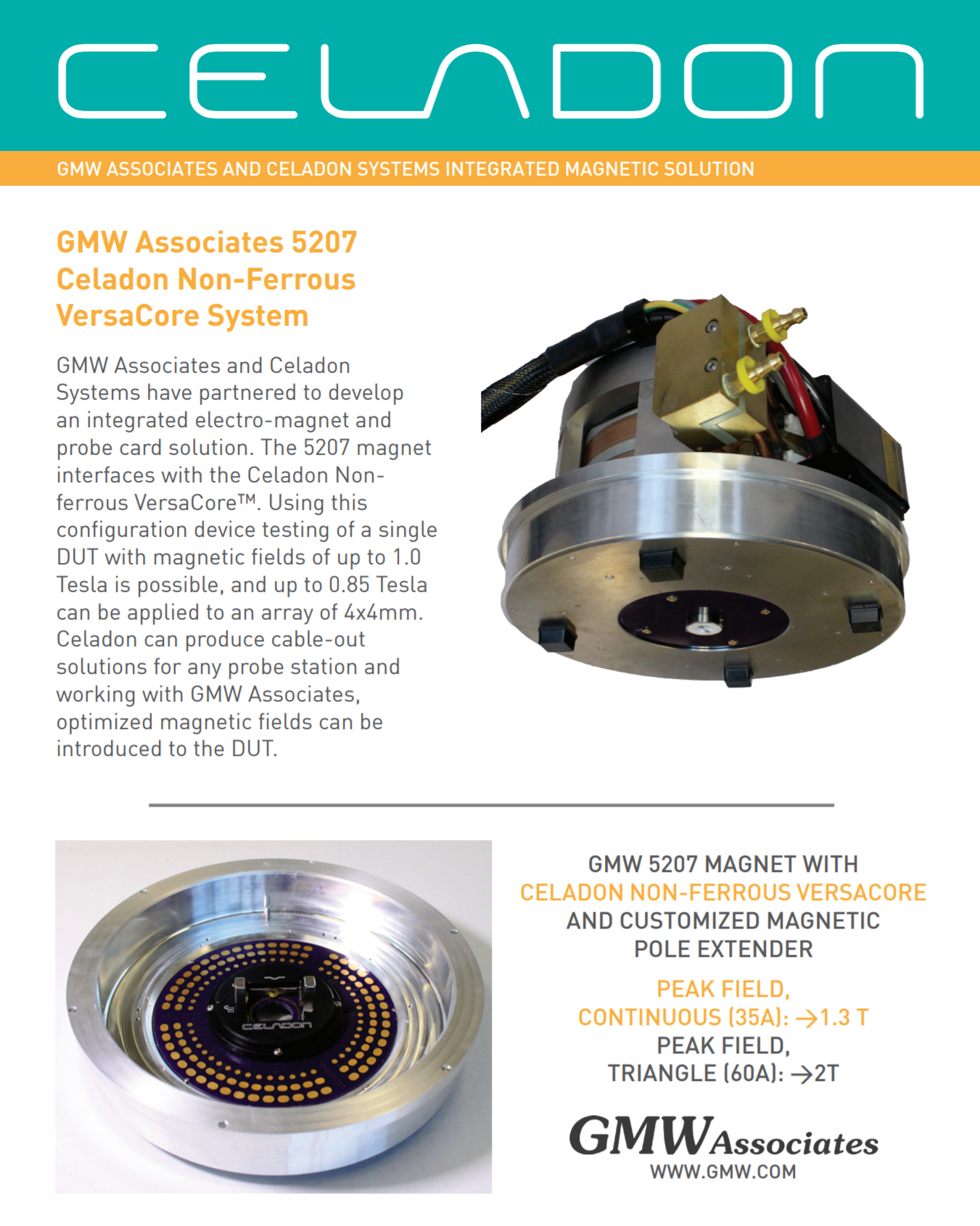
Celadon’s 3000V VersaJet™ System enables on-wafer probing from room temperature to 200C
Celadon Systems, Inc., the home of “Peace of Mind Probing”, has led the industry in high temperature on-wafer probing solutions for over 20 years. When it comes to high voltage testing, the key to success is arc suppression.
Celadon VersaJet™ System including the VersaJet™ Control Unit and Heater below
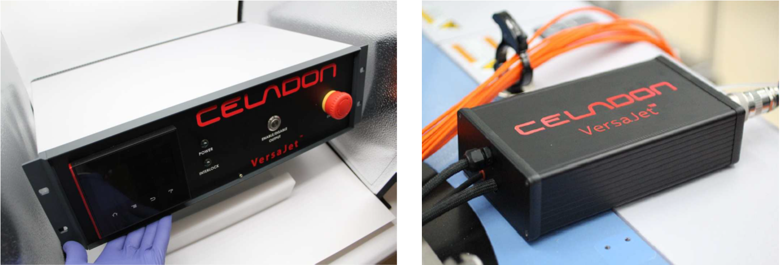
Celadon’s VC20EHV™ and 45EHV™
Celadon’s High Temperature, High Voltage solution consists of a VersaJet™ Controller and Heater, 45EHV 4.5inch Adaptor and VC20EHV Probe Card.
Celadon believes there isn’t a good reason for allowing hard break downs to occur when performing high voltage testing. Celadon’s high voltage team spent almost five years developing test wafers, test methodology, test equipment, and probe cards in an effort to reduce hard break downs. Several papers were presented at various conferences reviewing test technique and system performance. Click on the highlighted link to go to the papers: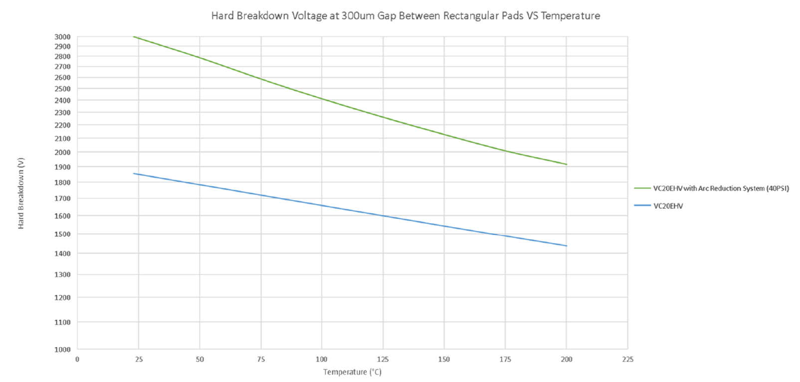
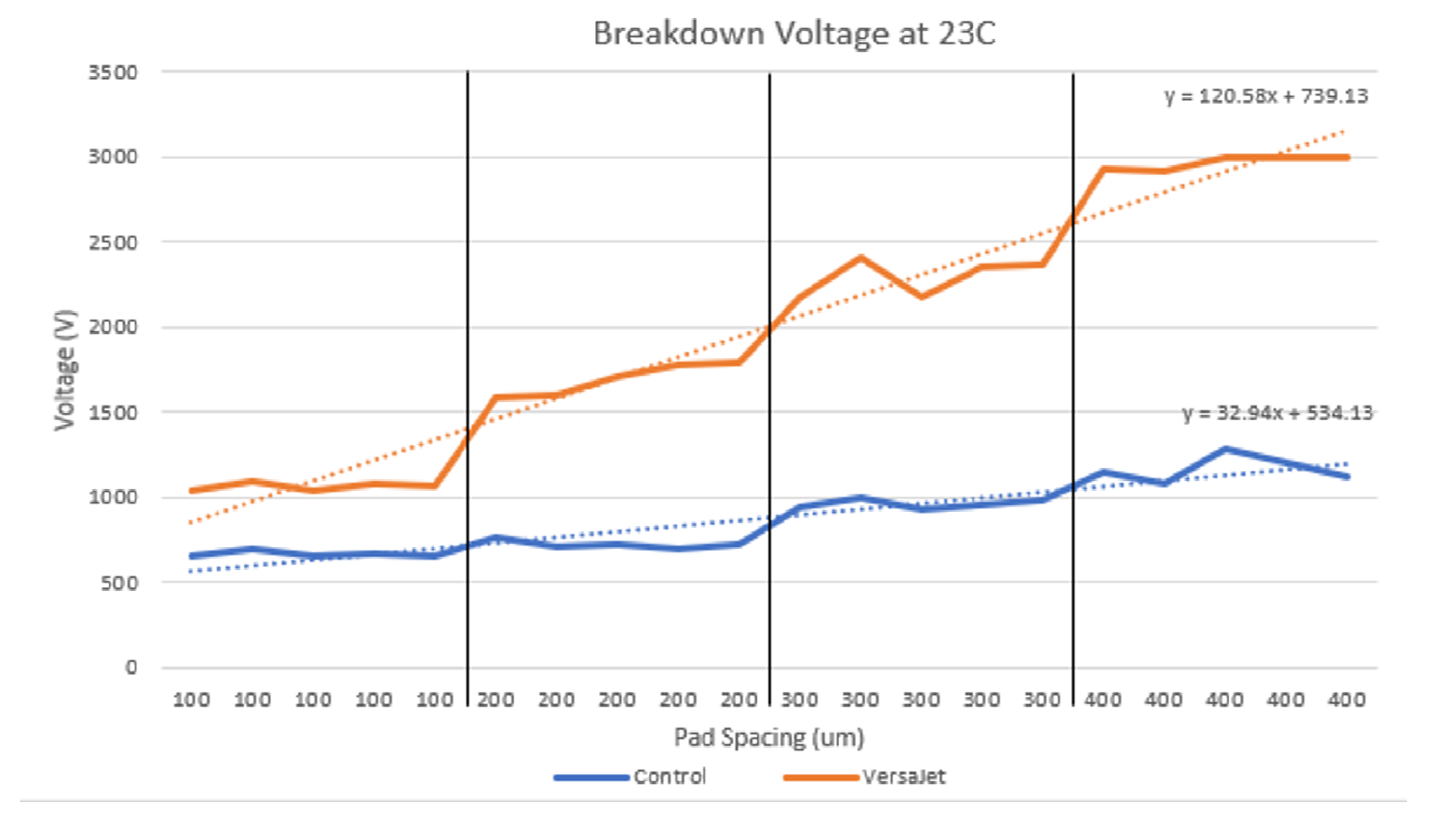
Cascade (FFI) Compass User Group, “Achieving 3000V at the Wafer Level”
SW Test, “Forget the Paschen and Embrace Turbulence”
The system is based on the popular and modular high voltage version of the VC20E VersaCore™ probe card. With pattern changes, the engineer will only need to change the VC20EHV probe card core, the rest of the set up all stays in place. This results in hundreds of hours saved in set up time.
System Overview
Here is the link to the High Voltage Product Guide
The system can support up to twelve 3000 Volt channels and 32 fully isolated low leakage channels. Celadon uses a propriety insulative material which eliminates the risk of probe beam to wafer arcing.
The VC20EHV (high voltage probe card) and 45EHV (high voltage 4.5inch adaptor) are both required in the high temperature and room temperature setups. For a room temperature set up, Celadon offers a kit that includes a regulator with a display and house air interface. This setup can extend the breakdown voltage at room temperature 50% or more as shown in the graphs below.
For high temperature testing, the VersaJet™ Controller and Heater are required for arc suppression. The air lines and electricals coming from the VersaJet™ Controller run through the VersaJet™ Heater and then are snapped into the back of the VC20EHV probe card while mounted in the 45EHV adaptor. This air stream is temperature controllable by the VersaJet™ Heater. Matching the VersaJet™ air temperature to the chuck/wafer temperature helps maintain stable DUT temperature for more accurate measurements. This connection at the VC20EHV probe card includes a safety interlock as well as air supply and thermal feedback sensors.
The directed air coming from the cap that is snapped into the back of the VC20EHV disrupts the ionization path and produces a high pressure “air bubble” at the wafer surface. This “air bubble” prevents surface arcing or die to die arcing, which can extend the break down voltage up to 50% at temperature.
Installation Example:
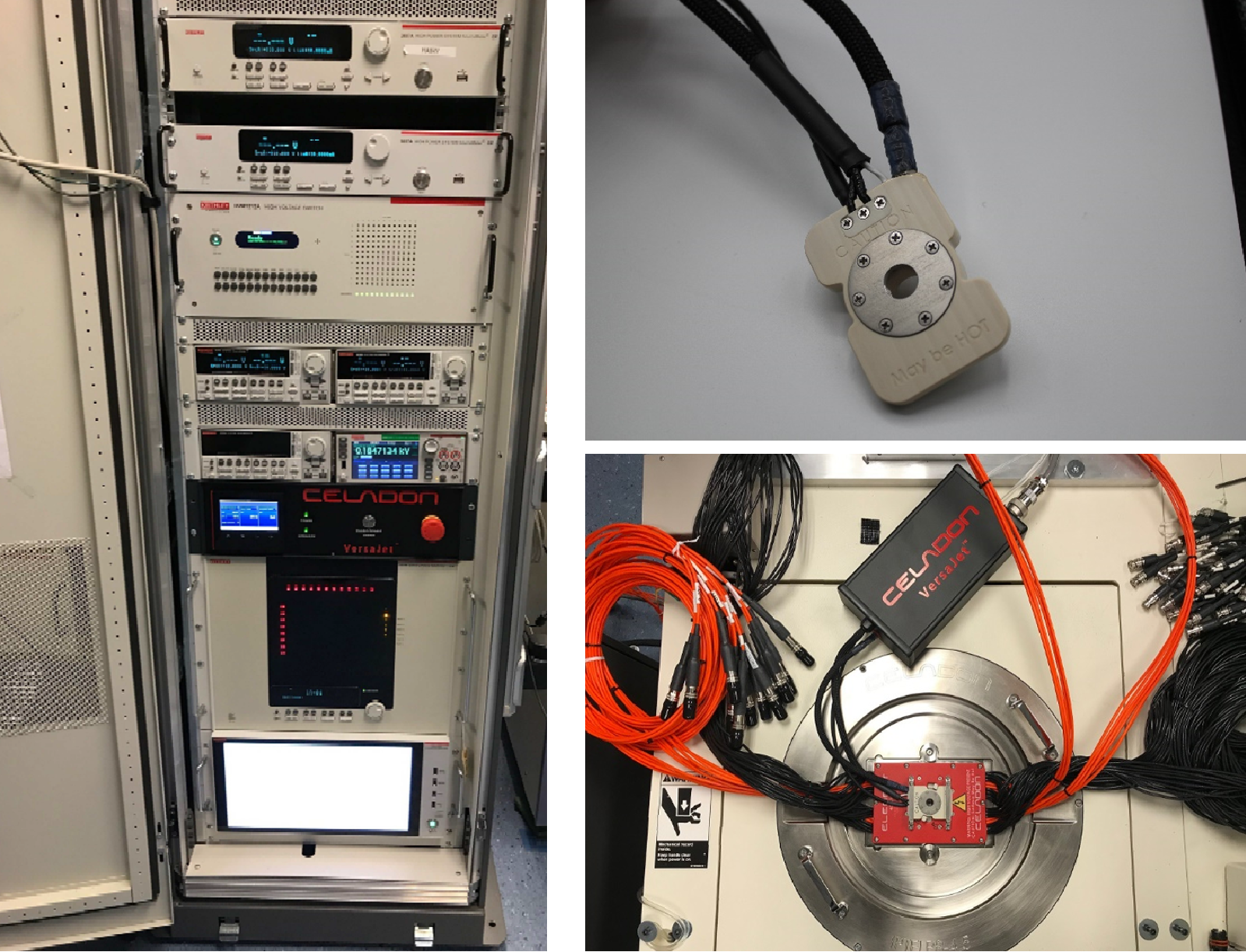
Celadon’s VersaJet™ Installed in a rack, the VersaJet™ heater, 45EHV and VC20EHV installed in an auto-prober setup.
If you are challenged with on-wafer high voltage probing, please reach out to salesteam@celadonsystems.com, we are happy to support you.
Celadon Systems, Inc., is a US based industry leading on-wafer probing solutions provider focused on the design and manufacturing of advanced probe card solutions and high-performance cables.
April 30, 2020
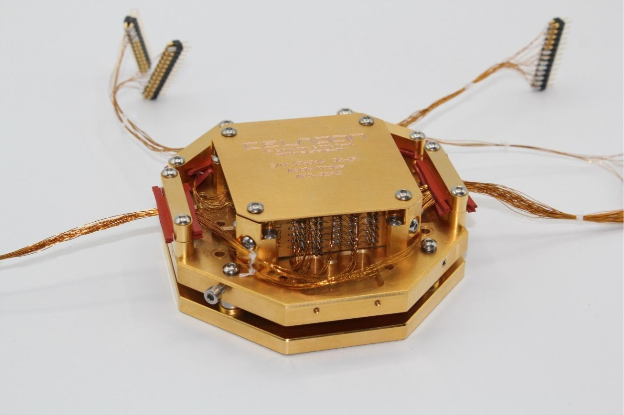
Celadon Cryogenic Probe Cards – Probing extremely small pads with and without a Prober at 4K
Celadon Systems, Inc., the home of “Peace of Mind Probing”, has been a critical supplier of advanced Cryogenic Probe Cards to Quantum Computing, Medical, Space and Military companies for over 20 years. These specialized cabled-out probe cards can be used down to 77K, 4K, or in some cases as cold as humanly possible.
Here are some examples:
Celadon’s Cryogenic VersaTile™
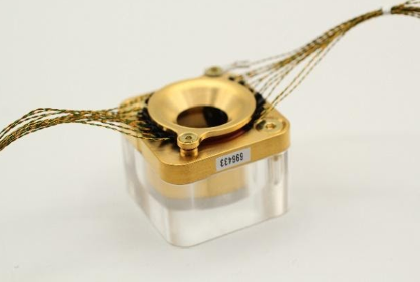
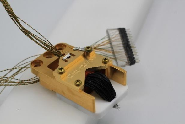
Celadon’s VersaTile™ has successfully probed at 6×9 micron test structure at 77K.
Celadon’s Cryogenic Tile-on-Card™
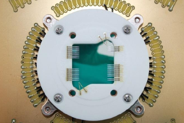
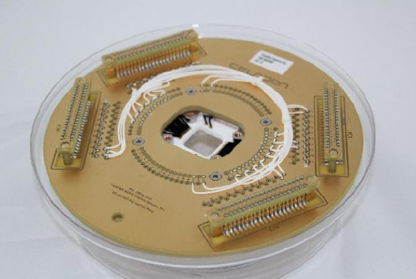
Celadon’s VersaTile™ and Tile-on-Card™ product families are compatible with most commercially available cryogenic probers. These cards were able to support 18 micron pitch.
Celadon has spent years researching and testing different materials to achieve stability over temperature at these extremely low temperatures. It is essential to find materials that are compatible and don’t compete with one another at temperature. If the Coefficient of Thermal Expansion (CTE) is too different between connecting parts on a probe card, cracking and breakage of part(s) can occur when going cold. When probe card materials’ CTE’s are not in equilibrium, one can expect a mess on their hands as materials can shatter at temperature.
Celadon invented the MobileProbe™ to support customers who have a cryo chamber but do not have a prober available to them.
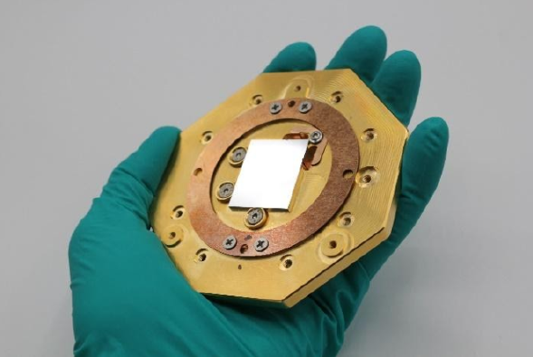
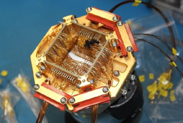
The MobileProbe™ includes an integrated probe card which enables single die probing [post-dice]. This unit can support hundreds of probes. The MobileProbe™ enables testing at 4K. This technology is also designed to be capable of scaling to test multiple diced die, or even 4 inch and 6 inch wafers.
If you are challenged with probing at Cryogenic temperatures, please reach out to salesteam@celadonsystems.com we are happy to support you.
Celadon Systems, Inc., is a US based industry leading on-wafer probing solutions provider focused on the design and manufacturing of advanced probe card solutions and high-performance cables.
Celadon Systems, Inc. provides business update on March 24, 2020
Friends and Colleagues,
We certainly hope you are all staying safe and well during the COVID 19 health crisis. As a critical supplier to many of you, please know our team is working hard to maintain business continuity. Our team implemented swift changes over the last two weeks to ensure our workforce is safe and healthy while adhering to the State and Federal mandates. Our support personnel and engineers are now working either full or part time from home. For now, Celadon is currently not accepting visitors on-site and our sales team will support our customers via teleconferences to keep our employees and customers healthy.
Celadon’s manufacturing team is up and running close to full capacity; the good news is we are building most product within our standard lead times.
In anticipation of a potential full shutdown should the state or community go into a two week full lock down and/or there is illness at the factory, Celadon would like to be proactive and work closely with our customers to ensure continuity. Please reach out to salesteam@celadonsystems.com to work out a support plan. Celadon is dedicated to serve our customers and will do our best to support you during this critical time.
#workfromhome
#staysafe

Kind regards,
Karen Armendariz
President and CEO
Phone: + 1 972 998 7091
Karen.Armendariz@celadonsystems.com
Celadon Systems, Inc.
13795 Frontier Court
Burnsville, MN 55337-4874 USA
Celadon Systems, Inc. Selects Karen Armendariz as new President and CEO
Celadon Systems, Inc. announced today that its leadership team has unanimously approved Karen Armendariz as the company’s next chief executive officer and president. Armendariz, who currently serves as Celadon’s VP of Worldwide Sales, will succeed Bryan Root, the company’s founder and current CEO.
“I am honored to be carrying the Celadon torch leading an extraordinary team of people that live Celadon’s core values of Integrity, Invention, Innovation and Dedication every day,” said Armendariz. ”Celadon Systems, known for providing unrivaled lab to fab probe card solutions that thrive in extreme environments, has been instrumental in equipping the semiconductor industry with probing solutions to successfully release new and reliable products for over 20 years. Today, Celadon Systems is uniquely positioned, with the most robust probe cards available, to enable the semiconductor industry to significantly reduce cost of test in production. I am thrilled to be given the opportunity to lead this exceptional organization determined to operate with excellence and provide the industry with unparalleled, leading edge probing solutions. “
As a member of Celadon’s leadership team since she joined the company in 2013, Armendariz has played an integral role in the company’s growth and success.
Armendariz holds a Bachelor’s degree in Electrical Engineering from the University of Oklahoma and an MBA from Oklahoma City University. Prior to joining Celadon in 2013, her history in the semiconductor industry included positions in operations and engineering management, in addition to her extensive sales and marketing experience.
Root, who started Celadon in 1997 with his wife Valerie, expressed confidence in his choice, “Karen’s reputation of strong leadership is well-known both inside and outside of Celadon. Her commitment, together with her industry experience, customer focus and strategic vision, makes her uniquely qualified to lead Celadon successfully into the future.”
For inquiries, contact Jennifer Nichols, Director of Finance and Operations, at jennifer.nichols@celadonsystems.com.
Celadon Systems is a privately held, 23 year old, US based manufacturer known for providing “Peace of Mind” probing solutions to the semiconductor industry.
Upcoming Trade Shows:
IEEE International Reliability Physics Symposium
Visit us at IRPS in Dallas, Texas
March 29 – April 2 2020
IEEE International Conference on Microelectronic Test Structures
Visit us at ICMTS in Edinburgh, Scotland UK
April 6 – April 9 2020
Expo Electronica
Moscow, Crocus Expo IEC Pavilion #3, Hall #14
April 14 – 16 2020
Semiconductor Wafer Test Workshop
Visit us at SWTW in San Diego (Rancho Bernardo Inn)
June 7 – 10 2020
Semiconductor Wafer Test Asia
Visit us at SWTWA in Hsinchu Taiwan R.O.C. (Sheraton Hsinchu Hotel)
October 15-16 2020
IEEE International Electron Devices Meeting
Visit us at IEDM in San Francisco, California (Hilton San Francisco)